
Background
Microchannel Plates (MCPs) are typically used as an amplification stage in particle and photon detectors. They are comprised of millions of parallel micron scale diameter glass capillaries bundled into a two-dimensional array. Amplification occurs when a "primary" electron or other ionized particle strikes the wall of a pore and excites multiple "secondary" electrons within the material. "Secondary electrons" escaping the pore surface are accelerated in the electric field within the pore, eventually striking the wall, creating a cascade effect as the process continues down the pore.
Using a photon/particle counting imaging detector scheme is one of the best methods for characterizing MCP performance. These detectors can be used to perform a set of basic tests, including resistance vs. voltage, gain vs. voltage, gain and imaging uniformity, and the background uniformity and magnitude. They can be utilized during life testing and burn-in to provide feedback on proper illumination, enabling measurements of any changes in the uniformity or background. They are advantageous when quantifying the detection efficiency, allowing background reduction by selection of counts only within the illumination spot. This detector system will greatly improve the diagnostic capabilities at SwRI and enable many current and upcoming SwRI programs to better assess the performance of their MCPs, especially when the final instrument is non-imaging.
Approach
The objective of this program is to design, fabricate, and test a 100 mm × 100 mm imaging detector system for MCP characterization. The program was split into three primary tasks: development of a 100 mm cross delay line (XDL) anode, design and fabrication of the demountable detector hardware, and assembly and testing of the full system.
-
Detection of a photon or particle by an MCP results in a charge cloud that can be measured by a patterned anode. Delay line anodes encode the photon or particle interaction position by comparing the time difference between the signals measured at two ends of a serpentine trace. Cross (or double) delay line anodes utilize an orthogonal serpentine to encode the second coordinate position. The XDL approach was chosen due to its relatively simple design (a 4-layer board with 4 connections), existing readout electronics (a time to digital converter from Sensor Sciences), and good performance <100 µm spatial resolution expected).
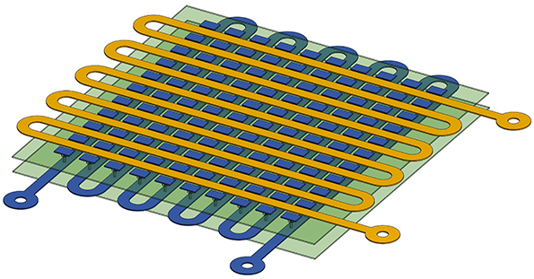
Figure 1: Example of the board layout (not to scale) showing orthogonal serpentines (yellow and blue) separated by ground layers (green). The buried serpentine is connected to pads on the surface to collect charge. Pads will have the same collecting area as the top serpentine.
-
The demountable detector design followed a commonly used detector built on a conflat vacuum flange. However, instead of using a large, heavy conflat, the detector was designed to integrate with the modular vacuum hardware from IdealVac. The mounting plate for the demountable detector was designed to replace a window in the 9" × 9" × 9" cube chamber. The size of the baseplate was 6.5" × 6.5", the MCP mounting hardware was 4.9" × 4.9", leaving room for four welded in SVH feedthroughs for supplying voltage to the MCP stack and enough outer edge for an O-ring gasket seal. The detector base plate also included four welded in SMA feedthroughs for passing signals from the anode.
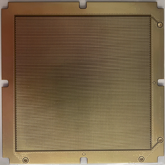
Figure 2: 100 mm × 100 mm cross delay line anode. The top layer shows a serpentine (x-axis) and pads with vias to a buried orthogonal serpentine (y-axis).
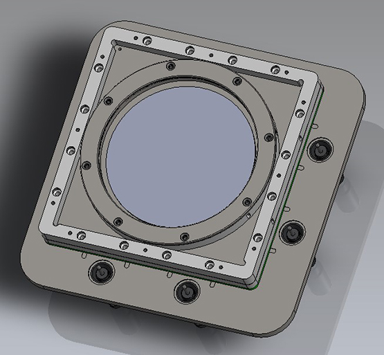
Figure 3: The demountable detector model. The base plate is 6.5" a side and the MCP mounting hardware is 4.9" as side. Shown here is mounting hardware for an 86 mm round MCP. The four pins (2 on the right and 2 on the bottom) are SHV connectors for applying high voltage to the MCP stack.
-
Performance evaluation of the detector hardware and anode were done using existing readout electronics from Sensor Sciences combining a preamplifier, a constant fraction discriminator, a time-to-digital converter, and an analog-to-digital converter. After initial setup of the gate and delays, the system generates an image, a gain map, and a pulse height distribution.
Accomplishments
This program successfully designed, fabricated, and tested a 100 mm × 100 mm XDL detector for MCP characterization with spatial resolution is <100 µm. The final detector hardware was assembled and found to be leak tight to <10-10 torr L/s with a helium leak tester. Four XDL anodes were fabricated, and benchtop testing found no shorts or opens. The performance characteristics (DC resistance, capacitance, and delay) were all in agreement with predictions. As a final test, a chevron pair of 86 mm diameter MCPs with 10 µm pores and 60/1 length to diameter ratio were installed and MCP characterization was performed using a mercury penray lamp (254 nm).
Figure 4: Photon image of a chevron stack or 86 mm diameter MCPs with 10 µm pores illuminated by a UV penray lamp (254 nm).
Figure 5: Gain map image of a chevron stack or 86 mm diameter MCPs with 10 µm pores illuminated by a UV penray lamp (254 nm). The gain map is the average gain per pixel.